Circuit Notes: A Budget Function Generator
I haven’t done a Circuit Notes post in a long time. Years, in fact! And I’m considering picking up a function generator as a very late Christmas gift to myself. So, naturally, I started poking around online for function generators.
There are some truly cheap options available - you can get kit versions on Amazon for less than $15, but these are pretty limited in bandwidth, scope, and specs. They’re basically just bistable multivibrators with some integrator stages for sawtooth and sine wave generation. One of these days, I’ll take a little time to look into those - there are lots of foibles that you can run into with these designs due to the analog imperfections in the capacitors and opamps.
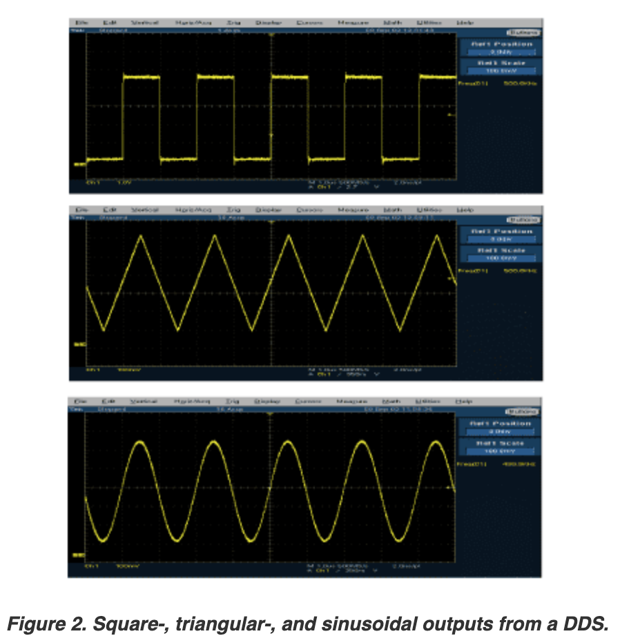
Today, however, I’m gonna take a look at the technology that rules the roost in function generation these days: direct digital synthesis. DDS relies on a packaged integration of a phase accumulator (fancy words for “an adding counter"), a lookup table of phase-to-amplitude conversions, and a digital-to-analog converter. DDS is another proof that digital technology makes certain subsets of electronics substantially easier: instead of a bunch of square wave oscillators and integration stages with the associated analog imperfections, you’re instead limited by the linearity of your DAC, the resolution of your lookup table, and the linearity of the output stage. Certainly not as high performance as a big, highly tuned analog function generator - but it does fit on a single chip!
If you want to get a halfway decent generator on the cheap, direct digital synthesis is the way to go. Analog Devices is the definitive market leader in DDS ICs, and they have plenty of great application notes that go very deep on DDS. (This article is a great intro that goes into much deeper detail than my brief overview.) Mix a convenient packaged IC solution with an explosion of electronic fab houses in China, and the result is a bunch of decent function generator designs popping up for sale online. Many of these designs are based around Analog Devices’ AD9834 chipset, so I decided to go deep on one of the designs I found resources for on Tindie. (I found a few decent teardowns of cheap Chinese function generators that are based around FPGAs with R-2R current mode DACs, but I didn’t feel like putting the time in to find detailed schematics of those systems.) Sadly, this exact product is no longer for sale, so I can’t get one, but I figured - why not take a look at the design, and see the gory details of how they did it?
You can find the circuit schematic here if you’d like to follow along. The results range from “moderately clever” to “not particularly pretty".
Schematic Wide Notes
I’ll break my analysis down section by section. Here’s a few notes for the schematic at large to get us rolling.
Why is this schematic so busy?
I can’t decide if I’m impressed that the schematic engineer managed to capture all of this information in one KiCAD page, or annoyed that they entangled so much together in a so little space. It’s tied together somewhat cleverly, but at the same time, this drawing is cramped! Did someone start charging these folks for KiCAD pages?
My personal philosophy is to try and isolate blocks of circuitry by function, rather than try to maximize density. I generally find that less is more when it comes to this kind of drawing. It allows me to think of each little functional sub circuit as a block with defined inputs and outputs.
Ah, well. Chalk it up to personal preference, I suppose.
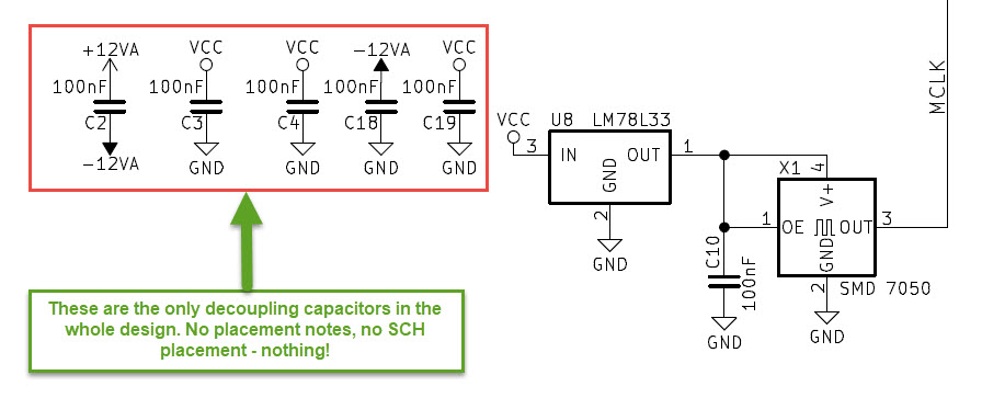
Where’s the decoupling?!
There are hardly any locally placed decoupling caps on this design! Most damnably, neither the DDS chip nor the output opamp have any sort of rail capacitance to decouple their current consumption. That’s a problem for both of these chips in particular, and we’ll dig further into why that’s a problem specifically for the DDS in a moment.
Generally, however, you need to include some sort of decoupling capacitor for any component that has a high instantaneous current draw. It turns out that most modern electronics meet this requirement in one way or another. The MCU in this design requires relatively large slugs of current at each clock cycle, when its internal registers and logic circuits latch over to the next instruction. Every opamp in this design is occasionally required to source an uptick in current when dealing with a fast transient. Switching voltage regulators depend on fast current transients to operate, and need excess capacitance to both store charge and limit electrical noise. (The maker did include caps on their boost regulator, but these are more on the bulk capacitance end. There aren’t many smaller caps to help control noise from this boost. More on that later.)
You need this charge stored locally, in a capacitor that is physically near the consuming chip. Proximity is critical - the voltage buses in the design have inherent inductance that tends to oppose fast upticks in current draw. A small capacitor placed near the pin acts as a little charge reservoir, with minimal inductance between it and the consuming chip. “Small” in this case refers to both physical size and electrical value. A physically small cap is easier to place close to the consuming chip, and minimizes parasitic rail inductance. An electrically small cap (picofarads for the closest caps) allows the cap to discharge more quickly - capacitance is a measure of the speed of charging and discharging, after all! Failure to include these capacitors can result in serious problems - noise on the voltage rail that couples into other circuits, or (in severe cases) a voltage glitch from a bus dipping too low.
The Direct Digital Synthesis IC
The AD9834 direct digital synthesis chip is the belle of the ball in this design. You can find a wealth of info on it on the Analog Devices Product Page. You can take a look at the other docs I referenced in the “Reference” section of this article.
No - seriously - where’s the decoupling?!
Since I’m working myself up to a nice little rant about decoupling, I’ll go ahead and say it again: damnably little attention was paid to decoupling the AD9834 chip. A cursory inspection of the datasheet says that only 8 capacitors are required in the chip implementation. Digging further into the datasheet, the “Layout and Grounding” section on page 26 reveals the following:
All analog and digital supplies should be decoupled to AGND and DGND, respectively, with 0.1 μF ceramic capacitors in parallel with 10 μF tantalum capacitors. To achieve the best performance from the decoupling capacitors, they should be placed as close as possible to the device, ideally right up against the device.
There is, to my eye, but one 10uF cap on the whole board, and it’s nowhere near the DDS. (It’s near the input LDO! Where it’s likely overloading that TI linear regulator. Likely, but not certainly - the LM78 family doesn’t appear to be one of those fussy low-dropout linear regulators that becomes unstable with too much output capacitance. That cap is, however, certainly slowing down the loop response of that regulator.)
A bonus musing about decoupling: I can’t help but wonder if any additional decoupling or filtering would improve the quality of the analog output here. Since AVDD and DVDD are sourced from the same rail in this design, it’s possible that some of the voltage noise referred to the DVDD rail by the digital circuitry might sneak its way into the AVDD rail, and, subsequently, into the analog output of the chip. Hard to say without a board in hand, but it’s possible that you could see a reduction in output noise by doing one (or all) of the following steps:
- Adding some decoupling to both the AVDD and DVDD rails,
- Adding some sort of higher frequency filter between AVDD and DVDD - a bead, or an RC filter with a small resistor and low corner frequency, or
- Separating the two supplies into separate regulators - the DVDD bus in this system could be served just fine by a switching regulator! Find yourself a nice low-noise LDO like the LT3042 to source AVDD, and Bob’s your uncle!
One last decoupling offshoot before we get to more interesting territory: regulator U8, and its load, oscillator X1, need some help. I’m not certain if the lack of input capacitance is a problem for U8 - TI’s datasheet for the LM78 series of linear regulators suggest that the input capacitor can be omitted if the part is within 3 inches of the upstream voltage source. However, TI’s datasheet does not cover the part number listed on the datasheet: TI doesn’t make an “LM78L33”. STMicro has a 3.3V linear regulator that appears to be a cross for this, but the part numbering is off by one character: the “L78L” series, rather than “LM78L”. The STMicro datasheet also doesn’t offer much in the way of guidelines for input or load capacitance as it pertains to noise or stability of their part. You could argue that the 0.1uF cap on the oscillator rail is serving the purpose of output decoupling for the regulator, but there are issues with that chunk of circuit as well. The load, oscillator X1, needs to get its power/reset priorities sorted out. An additional 100nF cap for the V+ pin, and a resistor to prevent OE from going high until after X1’s voltage rail has stabilized, would sort out any issues with that oscillator starting up correctly. Better yet - use one of those nice unused MCU IO to control the oscillator output enable. Then you can feel the heady rush of power as you give yourself complete software control over the AD9834 reset sequence!
The AD9834 Analog Stage
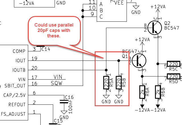
The schematic author has done some clever things with the analog output of the AD9834. I like the FSADJUST pin compensation with the BC547. I’d have to guess that helps a little bit with temperature compensating the BC547s in the output transimpedance stage. I was worried that it’s a bit too clever, but on closer inspection, I actually think it’s a well implemented hardware feature. For example, suppose we rail out the upstream offset reference of U4A to 5V, its maximum value. That divides down to $$5[V] * \frac{6.8[k]}{106.8[k]} = 0.318[V]$$ as an input for follower U4D. This sets an FSADJUST current of $$0.318[V]/2[kOhm] = 0.16[mA]$$, meaning that FSADJUST sees a total equivalent resistance of $$1.15[V]/0.16[mA] = 7.2[kOhm]$$. That translates to full scale output current of $$Iout = 18 * 1.15[V]/7.2[kOhm] = 2.875[mA]$$. This is precisely as it should be - a typical full scale output for the current driver is specified at 3[mA], with an absolute maximum output current density of 4[mA]. This follower/FSADJUST setting ensures that the AD9834 never gets close to sourcing that much current. That’s absolutely a good thing - the datasheet specifically warns about deviations in output voltage compliance above a 4[mA] current limit. Deviations in output voltage compliance == distortion! Distortion == bad!
The current driver outputs are also missing a 20pF cap parallel to the 220 ohm resistors. ADI recommends this in the datasheet to help keep clocking noise from sneaking into the downstream analog stage. Probably a good thing to have in this design, where you care about low-distortion analog output!
Board Analog Stage
We’ve taken a nice quick look at the AD9834, but now it’s time to turn our attention to the other major factor in this signal generator’s performance: the analog output stage.
Transimpedance Followers
This is one part of the design that the designer got pretty well right. The transimpedance stage is a nice little emitter follower that buffers and inverts the voltage developed across the 220 ohm load resistors. The followers, in this case, are a pair of BC547 NPN bipolar transistors. This has a couple of nice things going for it right off the bat - 220 ohms is a nice low resistance, which means they also have low Johnson noise. As a result, it will contribute relatively little voltage noise to the amp input - about $$1.88 [nV/\sqrt{Hz}]$$. Simplifying the input model to these buffers shows this really intuitively:
(insert picture: Norton equivalent of input to emitter follower)
We also have to account for this source resistance and the current noise of the BJT. This noise is the product of the source resistance, and the transistor’s inherent current noise - $$220 [ohms] * i_{n}$$. It’s hard to say with absolute certainty, as the datasheet of the BC547 doesn’t include much on noise specifications, but as most BJTs have an input current noise of single picoamps per root-Hertz ($$[pA]/sqrt{Hz}$$), it’s not an outrageous bet that this will be below 1 nV/rt-Hz.
What about the voltage noise of the BJT? You’ll note that the bias current of these transistors is pretty high - $$\frac{-11.4[V]}{2[kOhm]} = 5.7[mA]$$. This is because the voltage noise of a BJT amplifier decreases as the BJT’s collector current increases. This is to decrease the shot noise associated with the emitter resistance of the BJT. This is a purely fictional resistance - it describes the current/voltage relationship from the collector to the emitter. Decreasing the emitter resistance means upping the bias current. The goal is to decrease this emitter resistance (and its associated noise) to the point that it is lower than the base resistance of the transistor. There’s nothing we can do to change the base resistance - as a result, it’s the limiting factor in the transistor’s noise voltage.
So, what levers do we have to pull to decrease the transistor’s overall noise contribution to the circuit? Guessing from the bias current and the low input impedance, I’m fairly certain that the transistor’s voltage noise is the dominant term in our sum of squares.
I wonder what could be improved in this design by switching to a different kind of transistor altogether. The BC547 has some tremendous advantages. It’s cheap, and it’s readily available from plenty of suppliers. It is not, however, a particularly low noise transistor. The BC547 datasheet indicates a worst case noise figure for the BC547 at about 10dB at 1kHz. (Not a typical value, but quite high!) I’d be curious to see if the output SNR improves at low signal levels by switching to the BC550C. It’s covered by the same datasheet, and has a much tighter guarantee of noise figure than the BC547. That’s a spec that can cut both ways, though. It might mean that the BC550 and the BC547 are the same die, but sold under different part numbers thanks to binning at the factory. Horowitz and Hill make mention of the BC850C, another npn transistor from the Fairchild archives, but call out this part in particular as having a base resistance of 750 ohms. That’s pretty high, especially when you consider that the base resistance is the dominant term for voltage noise, and thus, the dominant noise contributor overall.
A more impactful change would be to go with a different transistor altogether, with lower noise numbers. Judging from the curves on page 483 of The Art of Electronics, you might be able to get significant improvements just by swapping over to the 2SC3324 from Toshiba. The 3324 has a distinct edge on the BC547/550 in voltage noise, at the cost of a little bit more current noise. The sum-of-squares rule for noise means that this tradeoff is certainly a worthwhile one; the transistor’s voltage noise is the dominant term in the noise equation, and the ‘3324 has about five times less voltage noise than the BC547.
A caveat - this sort of transistor optimization pushes the noise floor to a very low noise level. How low? Low enough that the transistor can be expected to contribute about one microvolt of noise to the circuit across a bandwidth of 100kHz. The SNR of the DDS is rated at -60dB at 20kHz. This swamps the output noise of the BJT by almost three orders of magnitude.
So, yeah, this was all basically analog yak shaving.
Output Driver
This is actually a complex enough topic that it deserves its own blog post. I’m gonna take a mulligan and circle back on this one.
In the meantime - for the love of God, get a decoupling cap or two!
Amplitude/Offset Controls
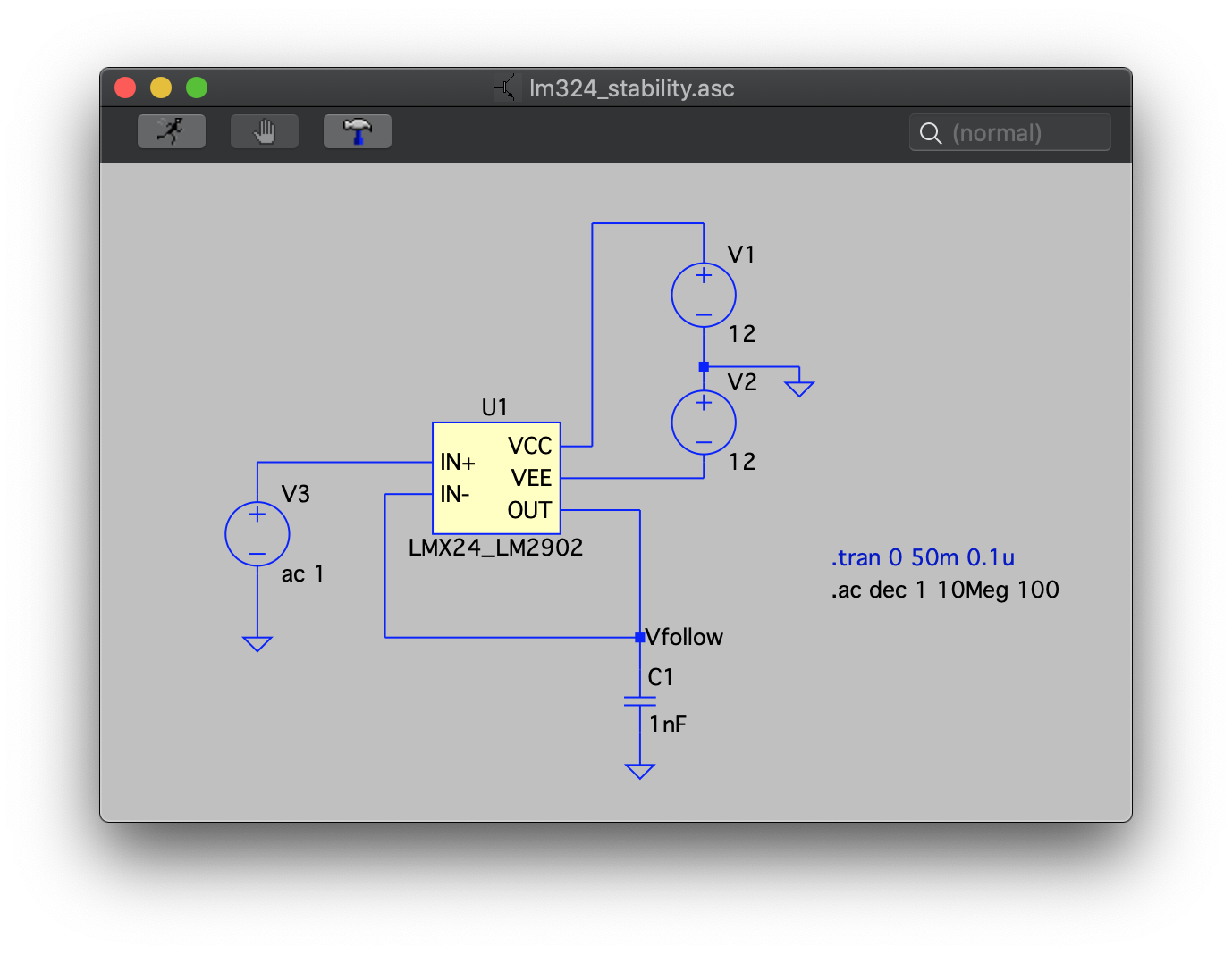
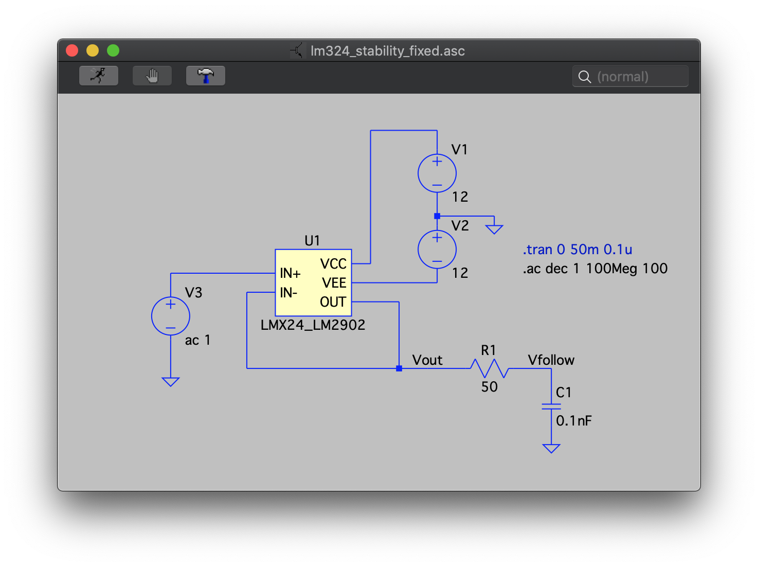
The amplitude and offset controls of this generator cook my meatballs. Why? Because this part of the design has opamp stability issues all day long!
For a start, let’s look at this brief excerpt from the LM324 datasheet - this shows the step response of the LM324 with a 50pF load:
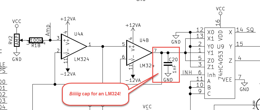
The 324 rings like a church bell with a 50pF capacitor load. This design saddles several LM324s with an output capacitance fifty times larger than that.
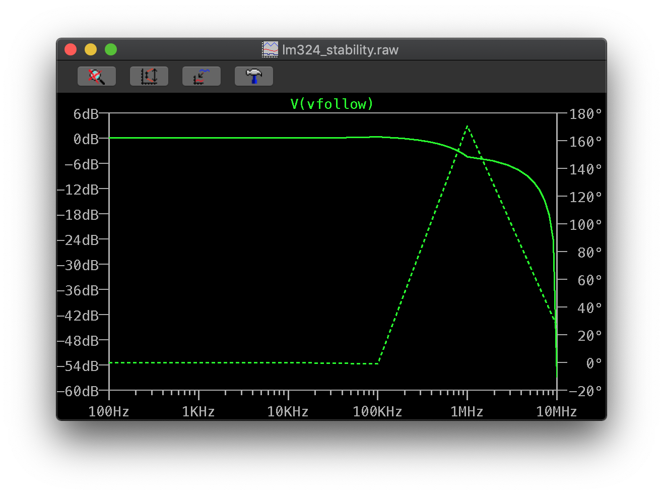
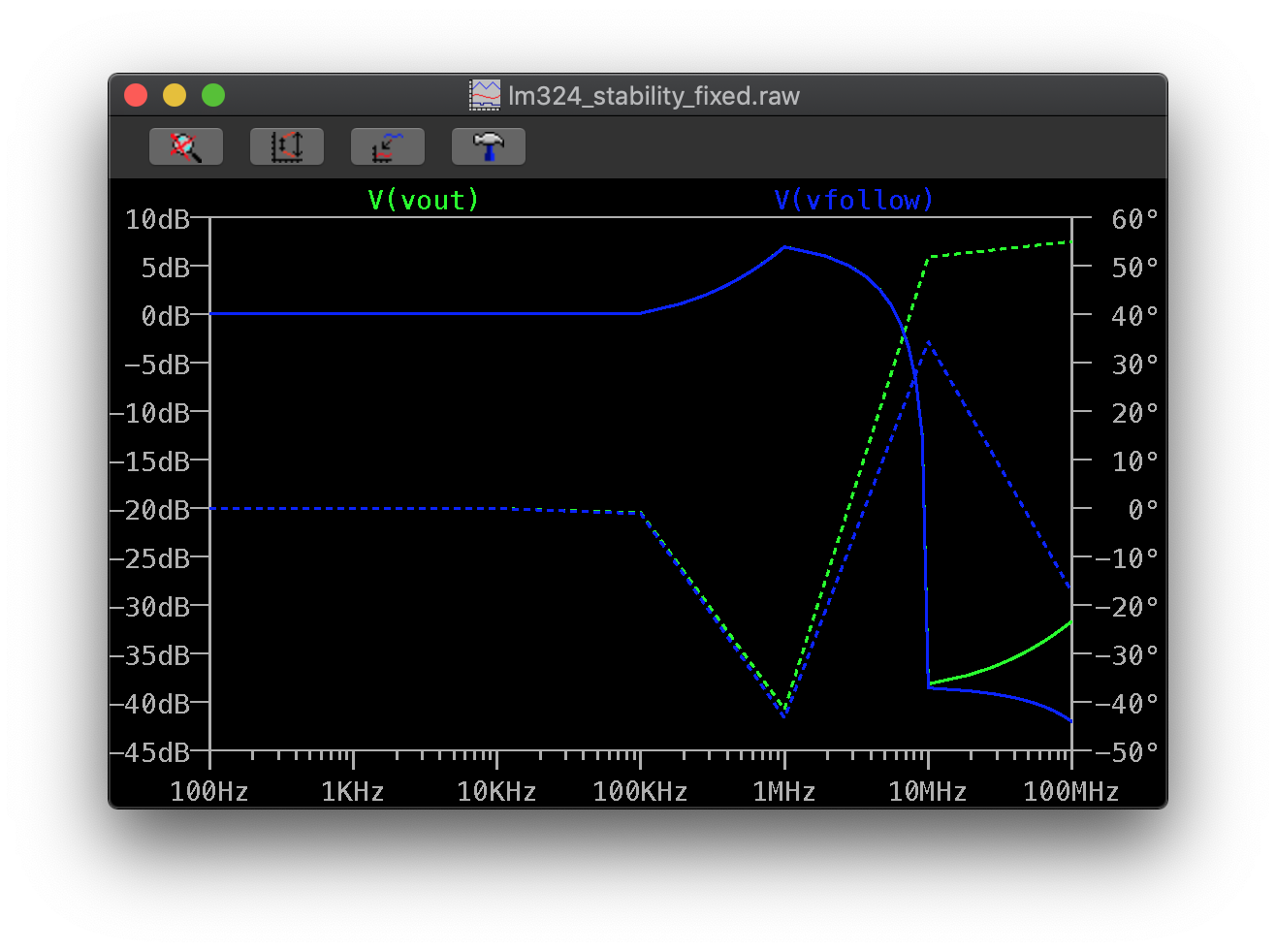
A quick plug into LTSpice should confirm that this isn’t a great decision:
And, predictably, a quick LTSpice sweep shows that this has precizely zero phase margin at 1MHz:
And, just for good measure, another quick LTSpice sim shows that the LM324 will start oscillating like mad in response to a 1uS step input:
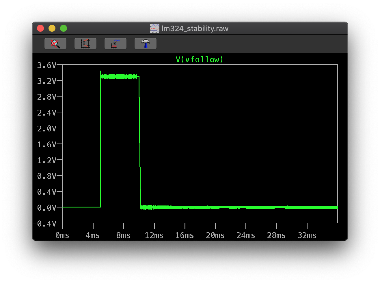
You could help yourself soften the transients on the input side of those followers by adding some capacitance to the opamp inputs. That will slow down the resulting output slew rate to match the new input voltage value. That’s a bad practice, however - the potential for instability will always be there, and once the opamp starts to oscillate, the cat is always going to be out of the bag! Case in point: look at what happens when the previous step response transitions back to a 0V offset. The LM324 continues to oscillate wildly around the ground point. There’s a 1MHz frequency stuck in the opamp’s feedback loop, with no way out!
Analog Devices has a zillion great app notes for helping stabilize opamp followers, but many of those solutions start to look like putting lipstick on a pig to me. The simplest way to fix this would be to just drop the value of the dang output capacitor! Decreasing it by an order of magnitude, to 100pF, solves basically all of the problems associated with this follower. The gain dive-bombs to about -40dB at 10MHz, with a solid 35 degrees of phase margin. Adding a small resistor between the follower output and the load capacitor helps bandlimit this voltage even further when necessary.
Square Wave Stage
I’m a little skeptical of the analog switching scheme used in the square wave output stage. From what I can tell, the design is using the sign bit output of the DDS chip to drive the switching terminals of the analog mux chip. The analog mux, in turn, switches its X output between ground, and whatever voltage U4B is set at. For all my skepticism, this is clever! I have a fondness for clever things. It has the benefit of inverting the 50 ohm output, as well as sending the output of X to the separate D header for digital outputs. It also allows for a full range of digital output amplitudes between 0-5V. It’s also kind of nice from a UX perspective. Only one BNC connector for all outputs is nice, and doesn’t beget any confusion to the hobbyist users of this generator.
On the flip side, this mux based switch is not a great output for testing digital circuits that need a fast edge. The analog mux switching is just too slow to provide a slew rate fast enough for devices that need CMOS-like transition speeds. Lots of cheap function generators online mention a “CMOS output stage” for just this purpose. I’d imagine there are some tradeoffs to this CMOS output stage - limited output voltages levels, no voltage offsetting, etc. I wonder what the “right” way to design a CMOS output would be, too. Would it be a single buffer/inverter, with an analog mux changing its input voltage? Or different buffer drivers with LDOs setting their input voltages?
Power Distribution
Now, for a quick word about the power electronics in this device.
Voltage Input
The barrel jack input is not half bad, but it doesn’t seem to consider input current to the board. I particularly wonder about the inrush to the 100uF bulk cap. How nicely will that inrush play with the 500mA fuse? What’s the i2t rating of the fuse?
On the bright side, it’s at least clamped to protect against reverse voltage - however, woe betide you if you plug in a -9V supply with a 1A output rating. Pop!
Additionally, I have one minor DFM concern - the reverse clamp diode, 1N4007, is NRND from Diodes Inc. I can’t tell if that’s just Diodes getting out of the business, or trying to sell more of their own S1M line.
Boost Regulator
This is basically just a lift of the reference design. Nothing wrong with that - that’s what reference designs are for! I am a little concerned about the delta between the input and output voltage. Will this generate excessive heat?
Also, to return to an earlier point - there’s not a lot of filtering of higher switching frequencies at either the input or output of the boost. That’s likely one noisy, noisy rail. Better hope those LM324s have decent PSRR!
The MCU
I’d first like to say that I’m surprised that STMicro hasn’t gone after this particular Chinese chip vendor yet. “STC Micro” seems a little close for brand comfort. That’s a lawyer problem, not an engineer problem, however.
Reset Circuit
This chip has an active-high reset line! Ain’t seen that in a while. The strapping deviates slightly from the reference design, but this should be OK - the reset input is Schmitt triggered, and likely high impedance. My guess is the builder was just trying to remove the need from the datasheet-recommended 10uF electrolytic cap on the reset RC circuit. That seems like it’s just throwing money at a component slot where it’s unneeded.
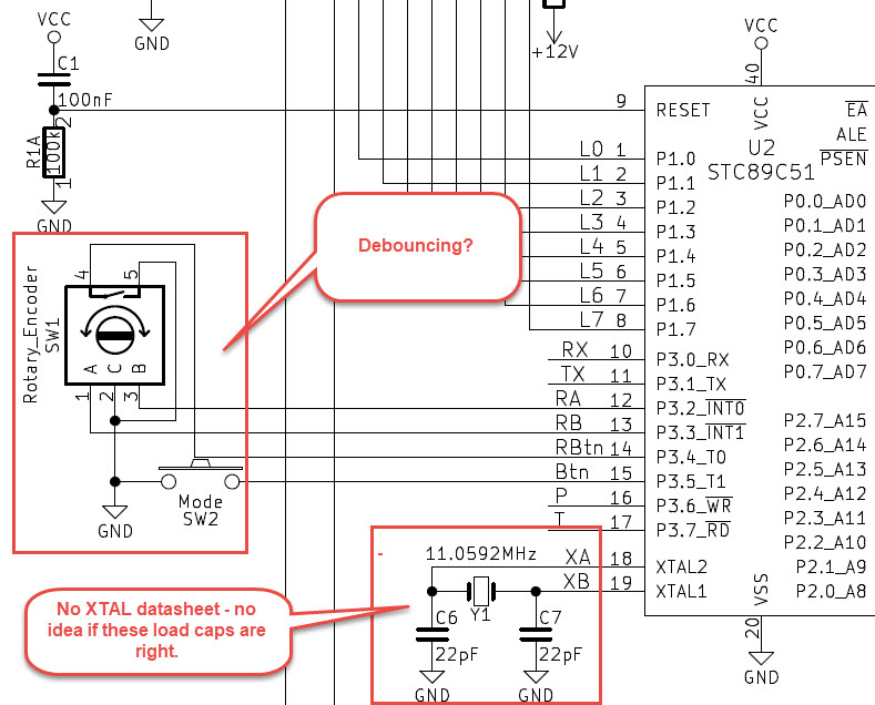
Crystal Circuit
Kind of difficult to determine whether these trim capacitors on this oscillator are right. There wasn’t a BOM included on the Hackaday.io file database - thus, I have no idea who this crystal was made by, or what its specified load capacitance is.
Also not clear from the source code what oscillator gain mode this MCU is running in. Fortunately, it seems like the default speed is slow enough that the oscillator doesn’t require an external feedback resistor to bias the oscillator driver.
Rotary Encoder/Button UI Input
No pull-ups or power to the rotary encoder to speak of. This might not be a problem - there could be internal pull-ups on the STC chip.
There’s also no sign of debounce in either hardware or software. Likely a problem!
MCU/DDS/LCD Interconnects
The layout files suggest to me that the route between the microcontroller and the DDS is pretty short, so unterminated digital lines are likely just fine here.
I’m not sure of how data is getting clocked into the LCD… unless the data line to the DDS is functioning as some kind of clock/write enable to the LCD. In which case, I retract my earlier statement - something multipoint is definitely going whack with the digital lines. Seems like that’s - well - not bad practice, but certainly not best practice. If you can deal with whatever weirdness is occurring on the clock path from the opposite transmission line route - why not? Probably saves some money on buffer circuits. Though I have to wonder - why would you choose a weird multiplexing scheme like that when you have an entire unused 8-bit GPIO port on your microcontroller? Maybe there’s only one SPI peripheral?
Conclusion
Well, that took a lot longer than imagined. So much for a relaxing design review over Christmas.
I’d be pretty remiss if I didn’t give a shoutout to Pulsar Labs for posting their design on Hackaday.io as open source hardware. For all the critique - this is a reasonably good design, and I’m a little bummed on their behalf that it is no longer for sale. (I’d also be interested in executing a pull request with some modifications to this, if a GitHub link were made available to the KiCad file.)
I included as many references as possible in the following section. If I screwed something up, omitted a detail, or got something wrong, feel free to personally message me at /u/LightWolfCavalry on Reddit. I eagerly await your comments, questions, and flamebait.
References
Further reading, if all that wasn’t enough for you.
Additionally - I’d like to call out the SnagIt screen capture tool, which I used to capture a few schematic images. We got a site license for SnagIt at work, and I ended up liking it so much that I paid $50 to get a copy for myself for home use. It makes screen captures and annotations a breeze!
- General
- All noise analysis notes inspired by the venerable The Art of Electronics (3rd Edition), by Paul Horowitz and Winfield Hill. Buy it from Adafruit! Or Amazon, if you must.
- AD9834 Direct Digital Synthesis Chip
- Analog Stage
- Reference/Amplitude/Offset Amps
- Output Amp
- AD811 Product Page
- AD811 Datasheet
- AD811 SPICE Model - Comes with a EULA to download
- STC Microcontroller