Quick Design Guidelines for Emissions Compliance
The design stage is always the best place to solve your radiated emissions problems. Here are some strategies that I’ve learned to keep your product designs emissions compliant.
Know your adversary.
When you’re talking radiated emissions, you typically care about one kind of measurement: the quasipeak. Bizarrely, I have met very few EEs that have even a passing understanding of what a quasipeak detector is:
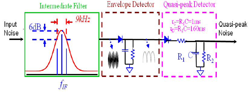
This is basically just a peak detector with a long hold time. In practical terms, that means two things:
- The higher in magnitude a signal is, the more it will charge up the QP detector.
- The more often a signal pops up, the less a QP detector will discharge between successive signals.
More bluntly: large currents show up on radiated emissions scans. So do frequently occurring signals, if they have a good antenna.
It’s all about current.
Radiated emissions is a game of Lenz’s Law, writ large. An AC current will generate a magnetic field. That magnetic field will radiate if it finds a suitable antenna.
Make sure you understand what the peak currents in your system are. Make sure you understand (or at least, have a good guess) of what path those currents take to get back to the source.
Put everything on one board.
Connectors are great radiators. Eliminate the need for them, and you eliminate the need to debug them. If you need a connector, however…
Keep the frequency low across connectors.
The risk of a connector is that it starts to act like an antenna when you shuttle high frequency content across it. If you need a connector in your system, the best thing you can do is to minimize its antenna risk. This means minimizing the high frequencies you send across it. If you keep your signal rates WELL under 30MHz, many of your issues will solve themselves.
As a corollary: you can get away with short bursts of high frequency signals across connectors, if they’re not happening continuously. The nature of a quasipeak detector means that a one millisecond burst of 20MHz SPI clock every second will have less of an impact than a constant 11.28MHz I2S clock. The same is true for power supplies. Be aware of how much current your peripheral devices are slugging down. Be aware of the duty cycle of that current. If something is rapidly cycling between low and high current operation, you will see it on a peak scan!
If you absolutely must run high frequency digital signals across a connector…
Choose connectors optimized for high frequency digital signals.
There’s no getting around it - sometimes you have to send high speed data across a connector. (You’re in this boat for sure if you’re working with card-to-card PCIe, or HDMI.) If this is the case, find a high quality connector that suits the purpose. It should have:
- good grounding
- sensible and regular grounding for return paths
- sensible pinouts to minimize current loops
- shielding (if possible)
If you’re dealing with a standardized connection (like HDMI, for example), there’s not a lot of wiggle room in these areas - the pinout is what it is. However, fine details like the quality of the shielding ground connection can have a significant impact on your final performance.
It’s the rise time, stupid.
AC currents are the root of all radiated emissions problems. All of the AC current in a digital signal is in the rising edges. Slowing down the rise time will decrease the AC current. I wrote about how to do this in some detail in the last post I wrote on radiated emissions.
The short version is that you should add in component locations for filtering your digital signals - a simple RC circuit can be enough in many cases.
Note slowing the rise time comes with a natural tension with regards to digital signal integrity requirements. It’s up to you to strike the right balance for the part you’re working with.
Keep your ground planes continuous.
The famous animator Hayao Miyazaki once sent Harvey Weinsten a samurai sword as a warning and a gift. To inspire Weinstein to not edit Princess Mononoke, Miyazaki included a short note with the gift: “No cuts.”
When designing your ground plane, you want to use the same mantra: “No cuts."
That means just what it sounds like: a ground layer should be one continuous plane.
That means:
- No slots.
- No cuts.
- No separate ground pours. (Your analog ground is not that special or necessary. Route all of the aggressors away from your super special analog traces. Still demanding your own ground? Route your analog ground as a differential trace instead of a pour.)
Why not? Every single one of those features has an opportunity to act like an antenna. If I can convince you of one thing in this post, it’s that you are terrible at predicting what structures in your product are good antennas.
Pay attention to the entire current loop.
Many engineers forget a fundamental engineering truth when designing electronics: current requires a loop to flow.
A loop of any size forms an inductor. An inductor of any size is going to create a magnetic field.
Currents in any device have two paths: the outgoing current sent via a signal or power trace, and the return current flowing back to the source. This is a big part of why we want a continuous ground plane: that allows a signal or power current to return to the source directly opposite the outgoing current.
If you don’t have a good path for the current to return to the source, it will find its own way back - typically, through something you don’t want it returning through.
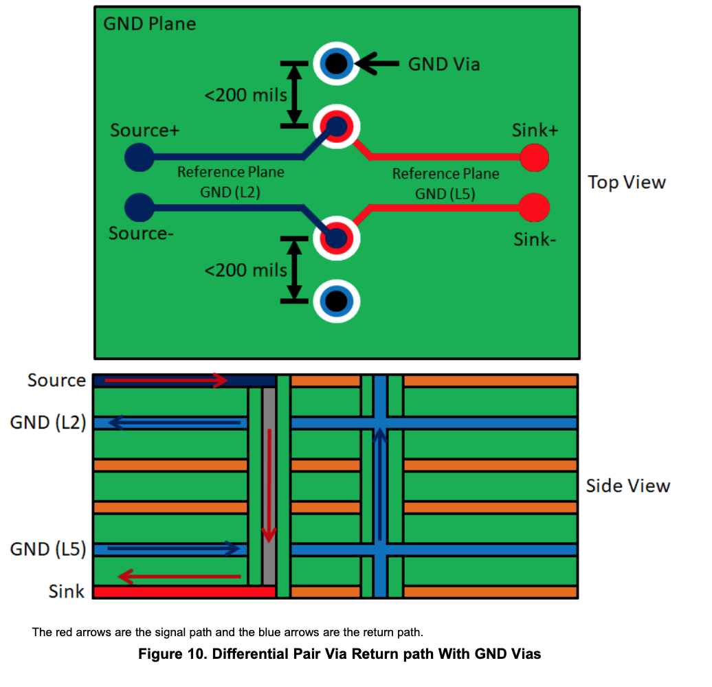
If you’ve got multiple ground layers, pay attention to your stitching vias. Make sure they are stitching your grounds together where a signal is swapping ground references. Here’s an example from a Texas Instruments app note on high speed differential routing for USB applications:
Keep high current traces short, and the current as low as possible.
What they lack in size or frequency, they can make up for in brute force of current.
One of the worst radiated emissions I’ve ever seen was for FET charge pumps in a Class-D amplifier. Each pump drove a peak current of about 4 amps to the downstream FET gates! Some additional series resistance made a huge difference in the radiated emission from the pump drivers!