NAND Flash: Dealing With a Flawed Medium
Introduction
Note: This is part 6 of a series I’m writing on NAND Flash. Want to start from the beginning? The first article is available here!
The last post in our NAND series probably left you wondering why we even bother using it at all. Between quantum mechanics, semiconductor variations, and statistical bad luck, there’s a lot that can go wrong with your bits. What’s the point of risking data in a medium that can go south at any minute?
As we mentioned in the last article, a lot of it comes down to price. If you want to fit 16 GB of data into a chip smaller than your thumbnail, NAND Flash is one of the only ways to do so at an affordable price point. Is the sacrifice of integrity a worthwhile one to make, however? With some common sense design techniques and a little help from software, the answer turns out to be a resounding yes!
Correct and Proper
The last article showed how data can get corrupted at any point during a Flash chip’s lifecycle. Reads, writes, and time can all affect data integrity. How, then, do we guarantee that the data stored in Flash is valid? The common solution is to use an error correction code, or ECC. The ECC functions as a check on the page data within a NAND device. It uses a fixed algorithm to generate an ECC value from a page of NAND data. During a write, this value gets stored in Flash along with the corresponding data. When that page is read back from Flash, it is run through the same algorithm to generate a second ECC value. If this second ECC value is identical to the original ECC value stored during the page write, then the data can be considered correct.
One of the most common coding schemes for guaranteeing NAND data is a Hamming code. A Hamming code depends on generating a set of parity bits from the data. A parity bit is a simple way of accounting for the number of binary ones in data. If the number of ones is even, then the parity bit is set as a one; otherwise, the parity bit is zero.
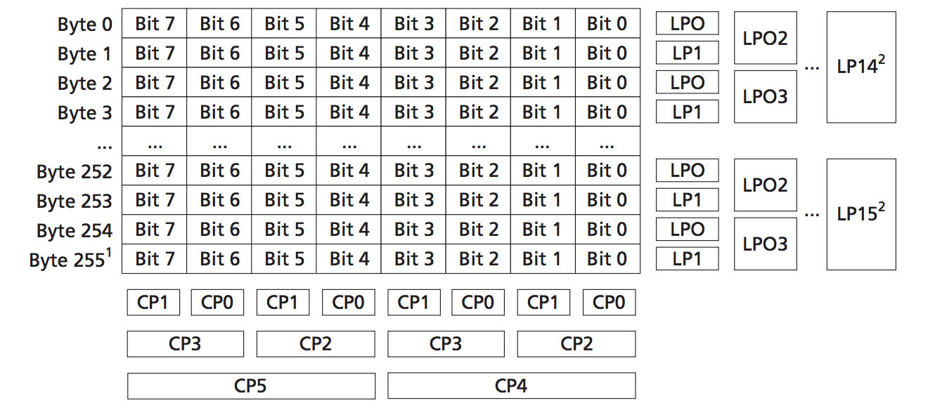
Hamming Code Generation (Courtesy of Micron Technology)
The diagram above shows an abbreviated method of generating a Hamming code for a 256-byte page of NAND data. This example shows how the parity bits of each byte (referred to as “line parity” in the example above) and each column are generated. Higher-order bits are generated by doing bitwise XOR operations on the lower-order bits (e.g. CP2 = CP1 ^ CP0; CP5 = CP3 ^ CP2;). This example of a 256 byte page will produce a 22-bit ECC value, which is stored in NAND as follows:
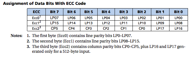
Hamming Code Byte Layout (Courtesy of Micron Technology)
What happens when your ECC values don’t match? As we’ve seen previously, there are plenty of ways for a bit to be wrong in a NAND Flash page. As you may have guessed, they’re called error correction codes for a reason - they can correct errors in paged data! Part of the brilliance of the Hamming code system is how simple it is to determine the source of the error within the block. The algorithm depends on XOR’ing the two ECC values. The resulting value can be interpreted as follows:
- ECC1 ^ ECC2 == 0: the two ECC values are equal; no error is present in the paged data or ECC value.
- Half of the XOR’ed bits equal 1: a single bit error exists in the page of data.
- Exactly one XOR’ed bit equals 1: a single bit error exists in one of the ECC values.
- Any other value: an uncorrectable error occurred.
Error correction codes provide a reasonably good system for catching flaws in NAND data. However, ECC is not without limitations. The Hamming code, while useful, can only detect two bit errors in the page used to generate it. Its correction capabilities are even lower - it can only correct flawed pages with one bit error! Any more errors than that, and the data becomes unrecoverable. There are more advanced error correction algorithms available now, but they generally come at the expense of requiring more bits for the ECC value. More modern algorithms like Reed-Solomon or Bose-Chaudhury-Hocquenghem (BCH) are capable of correcting up to twenty four bits within a page of data. They also tend to be very software intensive operations, and generally require specialized hardware acceleration to be used at a speed acceptable within most embedded systems.
Wear It With Pride
ECC is all well and good for preventing the occasional bit error in our data, but as a rule of thumb, the easiest errors to correct are the ones that never occur in the first place. With that in mind, it’s far and away better to design a system that minimizes the likelihood of bit errors whenever possible. How can we do this?
One of the first things we discussed in the last article was bad bit errors, where a floating gate dielectric breaks down to the point where it cannot store charge any longer. It turns out that the biggest culprit of dielectric damage in NAND is high voltage. But wait - don’t we need high voltages to program and erase NAND cells?
We’ve reached an interesting paradox here, folks - normal use turns out to be what breaks most NAND Flash. That means that programming and erasing a block is a relatively expensive NAND Flash operation; each cycle brings the device closer to the end of its serviceable lifetime. To counteract this, a technique called wear leveling is generally implemented. Wear leveling is really just a convenient term for spreading program/erase cycles evenly across the whole of a NAND device’s address space. Jim Cooke’s excellent presentation, The Inconvenient Truths of NAND Flash, illustrates the limitations imposed by single-block erase limits really nicely. I’ve recreated his math here with some simple calculations in a Python shell:
>>> pe_limit 	  = 100000	# Vendor-specified block program/erase lifetime
>>> daily_writes  = 1440	# Assumes one write/erase per minute (60 * 24)
>>> print pe_limit/daily_writes
69.44444
If we’re writing and rewriting a single block every minute, we’ll wear out that block in less than three months! However, if we distribute that across all blocks available, the math changes significantly:
>>> pe_limit 	  = 100000	# Vendor-specified block program/erase lifetime
>>> block_count	  = 4096  	# Total blocks in the system
>>> daily_writes  = 1440	# Assumes one write/erase per minute (60 * 24)
>>> print (pe_limit * block_count)/daily_writes
284444.444444
>>> print (284444.444444)/365.0
779.299
A simple wear-leveling implementation can extend our device lifetime from less than seventy days to over seven centuries!
Even though this operation is critical to the longevity of NAND devices, it’s still a bit of a pain to implement. We’re very used to using and reusing certain sections of computer memory over and over again, with no detriment to its performance. This approach clearly doens’t work for NAND Flash. Instead of using a single block over and over again, it’s far better to write new data into an unused block, and mark the previous data as invalid.

Wear Leveling Distribution (Courtesy of EECatalog)
To compensate for the limits in NAND Flash’s performance lifetime, specialized filesystems have been developed that allow for developers to see a continuous block of memory at the system level, while implementing wear leveling and other defensive NAND techniques at a lower level. A few examples of these embedded Flash filesystems include JFFS2, its successor UBIFS, and YAFFS, which is the filesystem of choice for Google’s Android operating system.
What Gets Measured Gets Managed
Even with all of these methods for preventing errors, NAND Flash is not a perfect technology. When bits in a block can no longer retain data correctly, we start treating that block as bad. We’ve seen that a block can become bad over time as it goes through repeated program/erase cycles. In addition, natural variations in semiconductor fabrication can lead to bad blocks being present in chips from the moment they roll off of the production line. Obviously, this has an effect on how we interact with the device - we need a strategy for bad block management where it’s easy to pick out the good blocks from the bad ones. Generally, the simplest strategy for dealing with bad blocks is to stop using them. To show that a block is bad, we have to update a region of NAND we have yet to introduce: the out-of-band area.

Page Dump of Small-Page NAND and OOB (Courtesy of HP)
The out-of-band region is a spare area at the end of each page of NAND Flash. It provides a special location to store metadata about the page - as you can see from the screencapture above, six bytes are allocated in this page’s OOB region to store the page ECC value. The sixth byte in the out-of-band region contains the bad block marker. If the bad block marker in the first page of a block contains any value besides 0xff, then the block is considered bad. (Note: The location of the bad block marker differs in certain NAND architectures - make sure you check the part datasheet for the correct location!) Since most NAND manufacturers allow themselves to ship Flash chips with a certain number of bad blocks, it is important to scan a chip for bad blocks before the initial programming occurs. It is also important to ensure that your Flash image is sized to include an appropriate bad block reservoir - a number of reserved blocks that would allow the image to fit into NAND even if the specified maximum number of bad blocks existed in the device.
Wrapping Up
The techniques listed above go a long way towards making NAND a viable nonvolatile storage medium. Admittedly, none of these are a silver bullet for making a perfect system. Understanding how your system uses Flash is critical to designing a system that will meet its lifetime requirements - you’re shooting for a design that can manage any user or runtime data effectively without loss or corruption.
As far as lowdown on NAND Flash goes, this just about wraps up what I’ve got to share on the subject! I hope you’ve found this series helpful - I’ve done my best to condense two years of work and study on the subject into a practical, easily digestible medium. I’m sure the fancy will strike to write on some more specialized topics as time goes on - stay tuned!
Like what you read? Got any ideas for what you’d like to read next? Shoot me a Tweet and say hey!
Further Reading
These videos from YouTube user Wayne Hamilton offer a great explanation of implementing Hamming codes on a byte of data. Part one shows how to generate the codes for a single byte of data. Part two shows how to correct a wrong bit in the byte.
Micron Technology, as you may have come to expect from previous articles, has an excellent technical note on implementing error correction in SLC Flash. I should also mention, by way of citation, that it’s the source of the Hamming code matrix and byte layout images I used in this article.
Though only indirectly related to NAND Flash, I would highly recommend reading up on Richard Hamming, the inventor of the Hamming code. Hamming is without a doubt one of the great modern mathematical geniuses; he was a veteran of the Manhattan Project and a longtime researcher at Bell Labs, where he developed the Hamming code algorithm in addition to numerous other pioneering works in mathematics.