NAND Flash: Device Architecture, Pt. 1
Introduction
Now that we’ve got the basics of floating gate operation under our belt, it’s time to talk a little more about how to string together a bunch of floating gates to make an actual NAND Flash IC! (If you’re not feeling so up on these concepts, have a look at part 1 and part 2 for a quick recap of how NAND Flash stores data.) We’ll start at the same level that we did in the previous article - the floating gate transistor - and zoom out from there.
A Bigger Byte
We’ve seen how to store a single bit using a floating gate transistor - it’s as simple as charging or discharging a floating gate. Unfortunately, one bit doesn’t do us much good as far as information storage goes. The good news is that it’s pretty easy to string together a bunch of bits to store multiple bit values - it’s just as easy as chaining multiple floating gate FETs together:
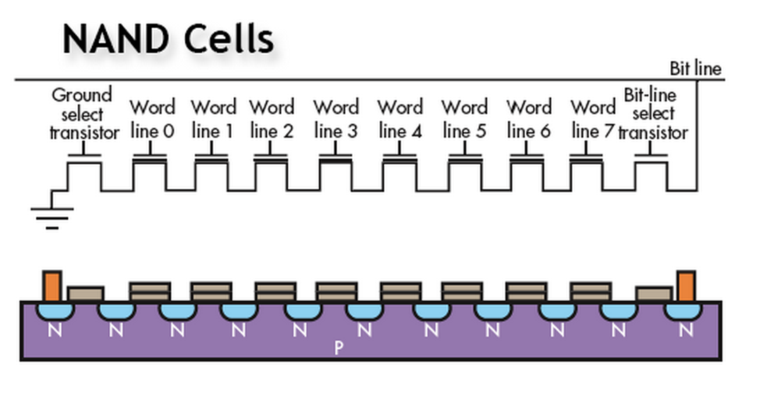
NAND Word Array (Courtesy of Toshiba)
As you can probably guess, this structure stores eight bits in eight separate floating gate transistors. This is a byte array - it contains an eight bit byte spread across eight transistors. Let’s say we want to read the value of bit 4 in this byte array. To read bit 4, you simply have to do the following:
- Set the voltage of control gate 4 low - that’s noted here as “word line 4”. Note that we’re not calling it a control gate any longer - we’ll see why in the next section.
- Set the voltage of all other word lines to a higher voltage than Vth, which we’ll call Vread. This is to override any possible charges lingering in the floating gates of the other transistors in the byte array - by cranking up the voltage at the other word lines, you are guaranteeing that the other transistors are turning on and giving you a good, low resistance connection to the bit line and ground.
- Set the voltage of the bit-line select and ground select transistors to Vth so we can connect the word array to the bit line.
- Read the value of the bit line. If there’s a charge on bit four’s floating gate, it will allow a channel to form in the P+ substrate before bit four’s transistor, meaning that the bit line will be connected to ground, and read as a zero. Otherwise, that transistor just looks like a high impedance, and will read as a one on the bit line.
And there you have it - in a mere ten transistors, we can store a whole byte of data!
Scaling Up
Well, we can store a byte, but there’s an obvious drawback here. If we store a byte using a byte array, we can only get at it one bit at a time. Luckily, this system of storing a byte scales pretty well. If we put eight of these byte arrays back to back, we can store eight different bytes independently, with each byte corresponding to a single word line.

Schematic View of NAND Array (Courtesy of InTech)
At this point, you have the most basic foundation of turning floating gate transistors into a big array of memory - the only limiting factor of this architecture is how much capacitance you can burden the sense amplifier of each bit line with.
Building NAND
At this point, you’re pretty familiar with this image of a floating gate transistor:

Simplified Side View of Floating Gate FET (Courtesy of EETimes)
While really nice for the purposes of explanation, this doesn’t look anything like a real floating gate transistor. In real life, those gates look something like this:

Silicon Side View of Floating Gate FET Array (Courtesy of Micron Technology)
Boxed in red are the structures that represent a floating gate transistor. Though this doesn’t look much like the nice, clean images we’re used to seeing, everything in this image maps pretty nicely to stuff we’ve come to understand conceptually. Section A shows the substrate, section B shows the control gate, and section C shows the floating gate. You can just barely see the oxide layers separating each of the silicon structures - thin, pancake looking deposits between each of the boxed layers. Note that everything you’re looking at here is really, really, really small in real life. In this picture, a centimeter corresponds to approximately 90 nanometers. For comparison, the minimum width of a human hair is generally 17 micrometers - about two hundred times the size of the structure shown here.
In the picture shown here, the neighboring transistors are actually the neighbors to the center transistor in its byte array. Each one of those stores a bit, and is storing each bit in space equivalent to much, much less than the width of a human hair. This is the crux of NAND Flash’s appeal in the market - you can get a ton of bits in a small space for really, really cheap.
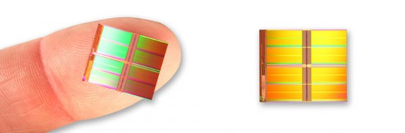
Photograph of a 16Gb NAND Flash Die, or 16*10^9 floating gates (Courtesy of Micron)
Pictured above is the raw silicon die that NAND Flash is built on. The finger gives you a nice sense of scale for how large it is - this is the structure that gets sealed up into a nice black plastic package and sent out to embed into all sorts of devices. Zooming in a level, we can actually identify some of the circuit structures from a high level:

Simplified Side View of Floating Gate FET Array (Courtesy of Micron Technology)
Wrapping Up
By this point in the series, you’ve probably got a reasonably good idea of how NAND comes together from its lowest levels to its highest. In the next post, we’ll discuss a bit more about how these architectural choices work out in terms of its operation.
Further Reading
While not pertaining directly to NAND Flash, one of my absolute favorite websites of all time is ZeptoBars, a Russian firm that specializes in chip deconstruction for the purposes of security analysis. Translation: they boil electronics in acid to take high-quality pictures of the silicon inside. A great resource on seeing what silicon looks like once you strip away all that boring black plastic.