bFunc - Project Journal - Week Four
Here’s the build log for week four of development for the open source function generator I’m trying to prototype and build in time for for OSHWA 2020.
Each day’s entry represents an hour’s work per day - the hour before I leave for my job every weekday morning.
This is my log for the week ending Feb 28, 2020. Here’s links to the prior weeks’ logs:
And, if you’re really into the philosophy angle, you can read up on the design doc for this project.
Also - I finally put all of my hardware and software source files on GitHub. Check ‘em out!
Feb 28 2020
- After some back-and-forth, CircuitHub has agreed to replace my boards at no cost. Wow!! Very impressed.
- Working today to evaluate the deltas between the design on my hard drive. I finally got to the point where I was convinced that everything is right, and pulled the trigger on shipping the updated board with CircuitHub.
- Highly recommend CircuitHub as a turnkey manufacturer stateside. They’re more expensive than China, for sure, but the workflow for reordering design is super slick.
- I did start looking at a few graphical KiCAD diff tools that show differences between schematics or layouts easily - it highlights diffs that it finds in bright, easy-to-see graphical overlays. It’s a tool I’ve always wanted at work for Orcad (which I’m coming to dislike more, the more I use KiCAD)
Feb 27 2020
- Really wanna make this thing work. Very cool tool. Could not get to run on my Mac. https://forum.kicad.info/t/net-aware-pcb-diff-tool-kicad-python-demo/12270/18
- No work otherwise - insomnia won.
Feb 26 2020
- You really need to stop making excuses, and start working on the USB portion of this. I demand that you download a reference implementation of USB, and get it running on your BluePill.
- Thanks for the nice note, Nash from Yesterday!
- Started a new directory to just make a vanilla USB CDC device with the Blue Pill.
- I selected Communication Device Class because: fuck it, I need to swallow my pride about using a better abstracted serial port.
- CDC is the only class of USB I really understand, and as far as I can tell, it suits my needs just fine.
- I don’t need synchronous transfers like an Audio Peripheral.
- I don’t need mouse/keyboard functionality, so HID is out.
- I probably will need firmware updates, but I don’t need them yet - so DFU is on the back burner for now.
- OK! First good sign! Building the default HAL settings seems to generate working code, which, in turn, yields a new USB device in my /dev/tty* directory.
- At this point, I got beset by some sort of wacky programmer error
- First, the chip failed to respond
- A quick GitHub check shows this issue, which might be what I’m seeing: https://github.com/texane/stlink#flash-size-is-detected-as-zero-bytes-size
- Although, after a few power cycles and resets, I was able to regain SWD communication but I don’t rightly know how
- Curious if I happened to set some setting wrong in STM32CubeMX - did I maybe select the wrong chip to try and program?
Nashs-MacBook-Pro:usb_cdc_demo nreilly$ st-info --probe

Found 1 stlink programmers
 serial: 343f72063447363360381257
 openocd: "\x34\x3f\x72\x06\x34\x47\x36\x33\x60\x38\x12\x57"
 flash: 0 (pagesize: 1024)
 sram: 20480
 chipid: 0x0410
 descr: F1 Medium-density device
- At this point I ended up spending most of my remaining time trying to figure out how to get the chip to respond again
- It appears to talk back now, after some combination of holding down the reset button and using st-util/st-info to get device info via SWD while the chip is held in reset and not executing the program in flash
- Now, however, I’m getting a second cryptic error:
Nashs-MacBook-Pro:usb_cdc_demo nreilly$ st-flash write ./build/*.bin 0x08000000

st-flash 1.5.1
2020-02-26T06:21:40 INFO common.c: Loading device parameters....
2020-02-26T06:21:40 INFO common.c: Device connected is: F1 Medium-density device, id 0x20036410
2020-02-26T06:21:40 INFO common.c: SRAM size: 0x5000 bytes (20 KiB), Flash: 0x10000 bytes (64 KiB) in pages of 1024 bytes
2020-02-26T06:21:40 INFO common.c: Attempting to write 12680 (0x3188) bytes to stm32 address: 134217728 (0x8000000)
Flash page at addr: 0x08003000 erased
2020-02-26T06:21:40 INFO common.c: Finished erasing 13 pages of 1024 (0x400) bytes
2020-02-26T06:21:40 INFO common.c: Starting Flash write for VL/F0/F3/F1_XL core id
2020-02-26T06:21:40 INFO flash_loader.c: Successfully loaded flash loader in sram
2020-02-26T06:21:44 ERROR flash_loader.c: flash loader run error
2020-02-26T06:21:44 ERROR common.c: stlink_flash_loader_run(0x8000000) failed! == -1
stlink_fwrite_flash() == -1
- Both of these symptoms are listed in the st-link GitHub page, but the only one with a quick proposed solution (mass erase, then try to reprogram) does not seem to fix it
- Theories:
- I accidentally set some security bit that makes flash inaccessible
- I overwrote one of my SWD pin lines to now be USB or some other function
Feb 25 2020
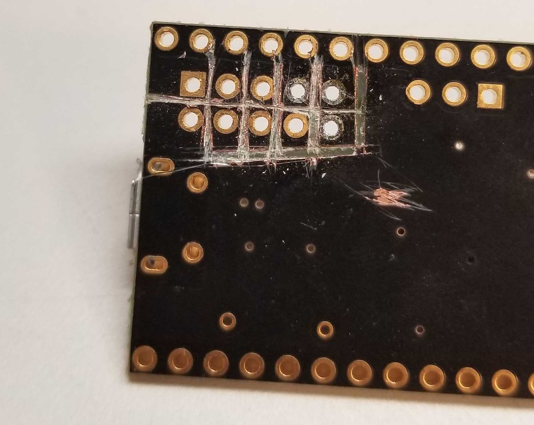
- Hardware
- First chunk of today is dealing with the shorts/fab error on J5.
- None of the pins of J5 were routed out on the bottom side of the PCB.
- As a result, all of the pins of J5 are shorted together, and to the bottom side copper plane.
- That’s extra problematic - that bottom side copper plane is GND, and the debugger connector has 5V, 3.3V, and connections to the debugger and the reset lines of the bFunc board.
- In short: it don’t fuckin’ work.
- CircuitHub’s been contacted, and I’ll be furtively swiping usage of a fancy microscope at my real job to take a picture of the fab error.
- Hard to do with a cell phone.
- Mental note: a good microscope is an essential investment for a home lab.
- I was able to do some further work at home by downloading my original PCB and SCH uploads from CircuitHub, back to my machine. The first thing I noticed was the fact that the PCB file downloaded from CircuitHub did not match the one on my hard drive. It didn’t have the proper voids around J5; it was also missing a few other minor tweaks.
- I think I’ve pieced together what happened from my memory here: I uploaded a set of SCH/PCB files a few days before ordering on CircuitHub to get a quote for board prices. In the meantime, I kept working on the PCB layout on my personal machine. Then, when I went to order PCBs, I made a stupid and critical error - I forgot to update the PCB upload on CircuitHub.
- There’s a special kind of stupid that you feel when you accuse someone else of making your mistake, and that is the kind of stupid I feel right now.
- Fingers crossed that nobody at CircuitHub is too upset by my dumb error. (Thanks for your help, Andrew and Robert!)
- Deleted the scratch PCB file “bfunc_layout.kicad_pcb”; I opened it while trying to debug this particular issue and found that it was an unused layout scratchpad. Could only cause confusion keeping it around at this point, so I deleted it.
- First chunk of today is dealing with the shorts/fab error on J5.
- Software
- Next step in software land: work on triangle wave generation.
- Damn - that was easier than expected!
- Three cheers for good state machine design!
- Square wave is going to be a problem in this eval setup
- I used a Sparkfun Minigen board as an AD9837 eval kit. (The real one from ADI was twice the price, and only worked with some SHARC or other ADI digital platform.)
- Downside: AD9837 is AC coupled. Don’t think that will play to well with square wave generation.
- I appear to be getting two back-to-back calls to SetWaveformMode() when only one will do
- A minor bug, but a bug nonetheless
- Next step in software land: work on triangle wave generation.
Feb 24 2020
- Lots of great feedback over the weekend on the project journal. Many great suggestions, particularly about trying out C unions to solve my problem of needing two names to point to the same chunk of memory. I think this ended up being the final winner:
struct ad9837_ctrl_reg {
    int freqreg   : 2;
    int b28       : 1;
    int hlb       : 1;
    int fsel      : 1;
    int psel      : 1;
    int reserved9 : 1;
    int reset     : 1;
    int sleep1    : 1;
    int sleep12   : 1;
    int opbiten   : 1;
    int reserved4 : 1;
    int div2      : 1;
    int reserved2 : 1;
    int mode      : 1;
    int reserved0 : 1;
};

union ad9837_dds_ctrl {
    struct ad9837_ctrl_reg reg;
    uint8_t data[2];
};
- I like it because it allows you to manipulate each bit with this nice struct interface, but then pass and transmit the underlying uint8_t data structure to the SPI peripheral when you need it. Who doesn’t love having the right tool for the job? 🙂
- So, this union seems to work right, except for one thing - it’s backwards
- Struct is packed in reverse order - all the bytes that used to transmit as 0x2000 now come out as 0x0004
- Reversing the order of the bits in struct ad9837_ctrl_reg does the trick!
- (Note - the code block above shows the correct order of the bits in the struct declaration.)
- Turns out this abstraction works really nicely for twiddling those same bits when manipulating the frequency register.
- Added a .gitignore file and removed all of the junk that spits out in the /build/ directory (no reason to upload that to GitHub!)
- Please, god, someone advise me on the right vim configuration to make this sort of shitty space formatting go away automagically
- BOARDS ARRIVED!
- …and they have problems. 😂
- The whole debug connector on the bottom side of the PCB is shorted together. All pins short to each other, and then to ground. 😫🤦♂️
- See below for a high grade microscope shot.
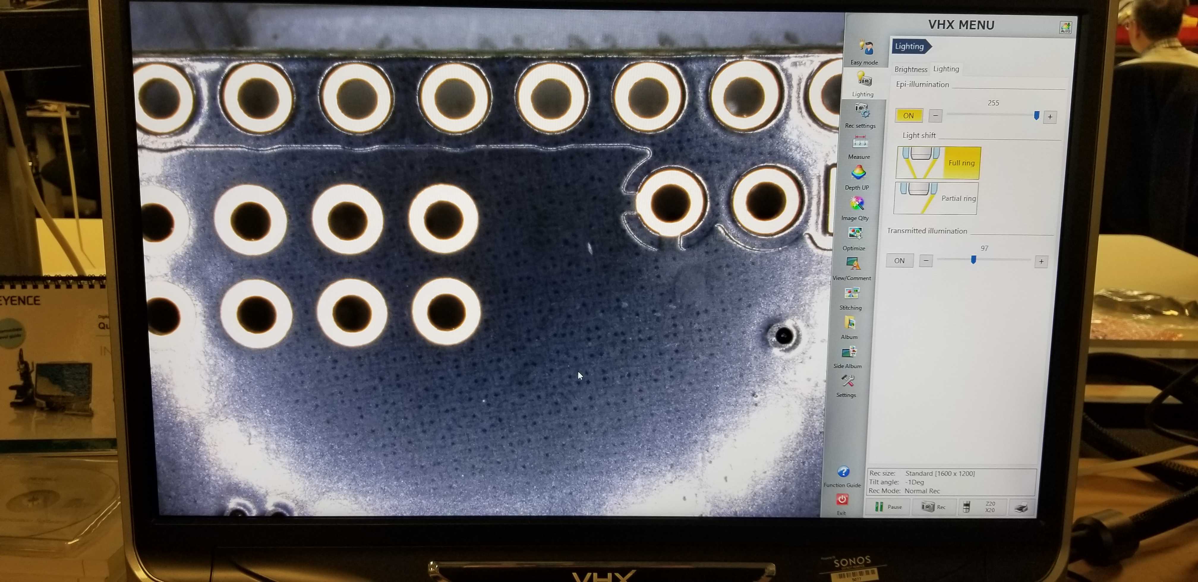
- Here’s what an hour with an exacto knife and a stereo microscope will get you (thanks, work!)